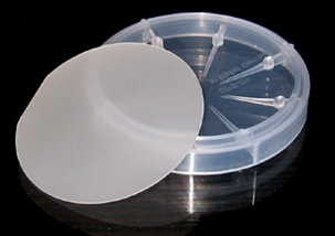
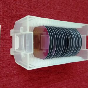
Description
P-GaN/N-GaN on Sapphire Specifications:
- Growth method :MOCVD/HVPE
- Conductivity : P-type/N+-type
- Dopant : Mg/Si
- GaN Thickness : 1-5 µm / 500nm-100 µm
- Concentration :>5E17 cm-3 / >1E18 cm-3
- Resistivity : < 0.05 Ohm-cm
- Surface :One side polished (SSP) / Double sides polished (DSP)
- Substrate Diameter :2’’/3’’/4’’ Sapphire wafer


Reviews
There are no reviews yet.