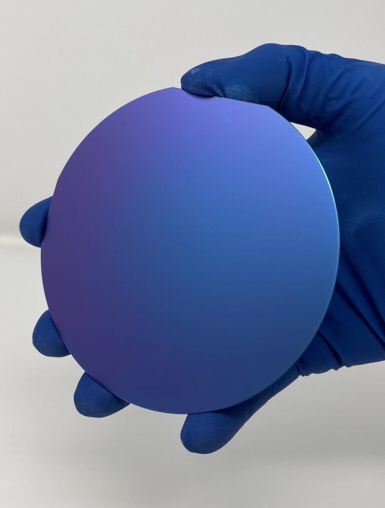
Silicon Dioxide (SiO2) wafers
Thermal oxide or silicon dioxide layer is formed on bare silicon surface at elevated temperature in the presence of an oxidant; the process is called thermal oxidation. Thermal oxide is normally grown in a horizontal tube furnace, at temperature range from 900°C ~ 1200°C , using either a “Wet” or “Dry” growth method. Thermal oxide is a kind of “grown” oxide layer, compared to CVD deposited oxide layer, it has a higher uniformity, and higher dielectric strength, it is an excellent dielectric layer as an insulator. In most silicon- based devices, thermal oxide layer play an important role to pacify the silicon surface to act as doping barriers and as surface dielectrics. We always choose prime grade and defect free silicon wafer as substrate for growing high uniformity thermal oxide layer to meet your specific requirements. Contact us for further information on price & delivery time.
| Specifications | Description |
| Oxidation Technique | Wet Oxidation or Dry Oxidation |
| Grade | Prime/Research |
| Diameter | 2 Inch-12 Inch |
| Oxide Thickness | 100-500 nm |
| Tolerance | +/-5% |
| Specifications of Si wafers | |
| Substrate Material | Silicon (Si) |
| Orientations | <100>, <111> & <110> |
| Si Conductivity | P-type / N-type |
| Si Resistivity | 0.001-10000 Ohm-cm |
| Surface | One side polished (SSP)/Double sides polished (DSP) |
| Applications | Semiconductor manufacturing, MEMS devices, sensors, optical coatings, microfluidics, etc. |


